
773700
Graphene, monolayer film
1 cm x 1 cm on SiO2/Si substrate, avg. no. of layers, 1
Synonym(s):
Single Layer Graphene Sheet
Sign In to View Organizational & Contract Pricing.
Select a Size
Change View
About This Item
UNSPSC Code:
12352103
NACRES:
NA.23
Product Name
Monolayer graphene film, 1 cm x 1 cm on SiO2/Si substrate, avg. no. of layers, 1
Quality Segment
form
film
feature
avg. no. of layers 1
resistance
600 Ω/sq
L × W × thickness
1 cm × 1 cm × (theoretical) 0.345 nm, monolayer graphene film, 1 cm × 1 cm × 525 μm, SiO2/Si substrate
General description
Graphene film
Growth Method: CVD synthesis
Transfer Method: Clean transfer method
Quality Control: Optical Microscopy & Raman checked
Size: 1 cm x 1 cm
Appearance (Color): Transparent
Transparency: >97%
Appearance (Form): Film
Coverage: >95%
Number of graphene layers: 1
Thickness (theoretical): 0.345 nm
FET Electron Mobility on Al2O3: 2; 000 cm2/V·s
FET Electron Mobility on SiO2/Si (expected): 4; 000 cm2/V·s
Sheet Resistance: 600 Ohms/sq.
Grain size: Up to 10 μm
Substrate
Size: 1.25 cm x 1.25 cm
Type/Dopant: P/B
Orientation: 100
Growth Method: CZ
Resistivity: 1-30 ohmcm
Thickness: 525 +/- 25μm
Front Surface: polished
Back Surface: etched
Coating: 300 nm thermal oxide on both wafer sides
Sheet resistance measurements were performed in a vacuum chamber to ensure their reproducibility, within a four-point configuration (van der Pauw geometry, silver paint contact) with injection of currents above 10uA
Graphene is a unique one atom thick, two dimensional allotrope of carbon. Among all the synthesis technique, chemical vapor deposition of graphene on various substrates is the most promising route for the large scale production of good quality graphene. Graphene deposited on dielectric surface may exhibit better performance in graphene based FETs. Graphene deposited on SiO2/Si may be deposited by direct chemical vapor deposition via a sacrificial copper film.
Still not finding the right product?
Explore all of our products under Monolayer graphene film
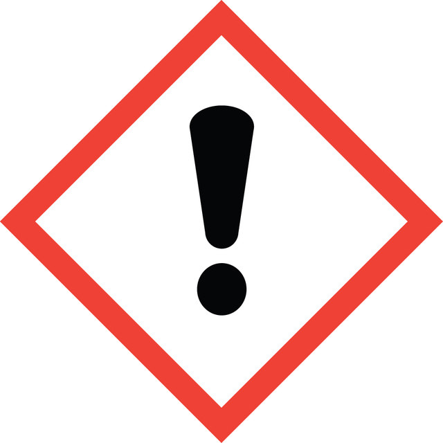
signalword
Danger
hcodes
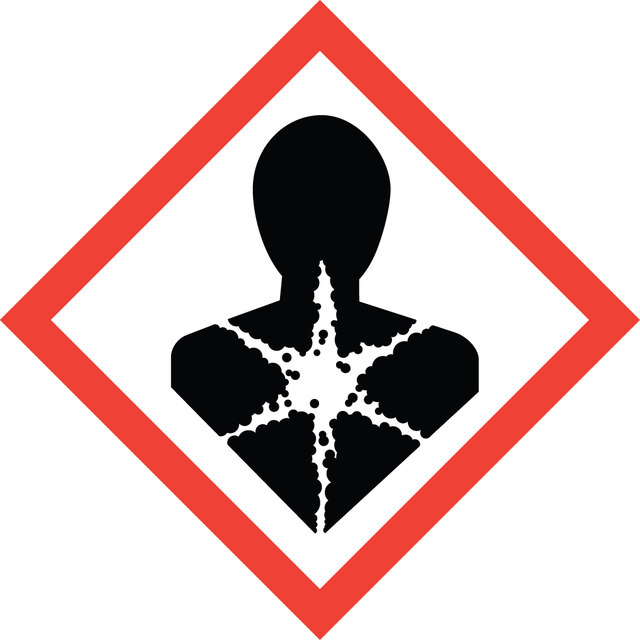
Hazard Classifications
Eye Irrit. 2 - STOT RE 1 Inhalation - STOT SE 3
target_organs
Lungs, Respiratory system
Storage Class
6.1D - Non-combustible acute toxic Cat.3 / toxic hazardous materials or hazardous materials causing chronic effects
wgk
WGK 3
flash_point_f
Not applicable
flash_point_c
Not applicable
Choose from one of the most recent versions:
Already Own This Product?
Find documentation for the products that you have recently purchased in the Document Library.